10W Three Stage Buck Convertor
General Use Three Stage Linear Voltage Regulator
Why?
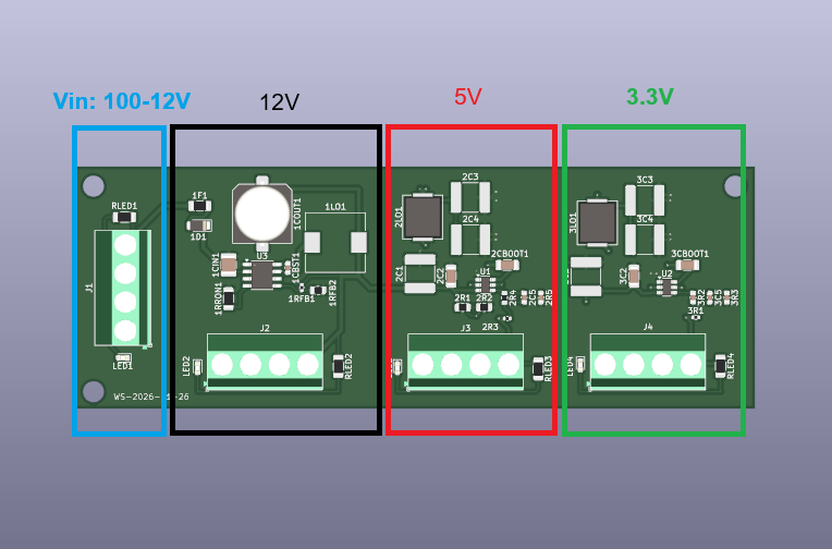
For my ESC Project I needed to support different voltages for different components. For example, the STM32 MCU is only 3.3V tolerant on most pins, the external DC cooling fan for the MOSFETs operates at 5V, and the MOSFETs for the power delivery have a Vgs of 12V. I needed a solution to efficiently convert my Vin (up to 100V) down to these voltages. I designed a simple test board using the LM5164 and TPS54302 chips before spending hundreds of dollars to manufacture the full ESC. This way I could also make layout improvements based on the feedback from this design.

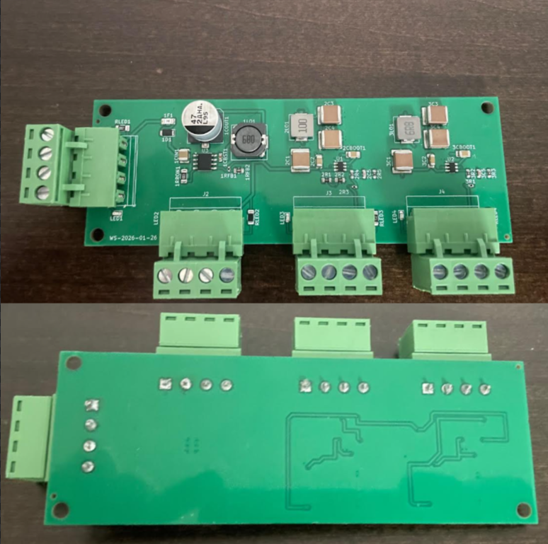
Finished assembly by JLCPCB

What?
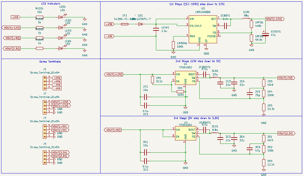
The board consists of the three stages, each centered around a buck convertor chip, some LEDs to indicate power and screw terminals for connecting to each output. The total output power of this setup is conservatively 10W (about 1A on the 12V stage, 2A on the 5V stage and 3A on the 3.3V stage).

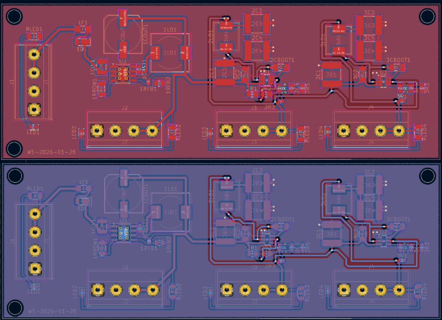
All of the components and most of the routing live on the top side of the board – that way JLC didn’t have to flip the board to solder components on both sides, saving me money. The board is two layers – more wasn’t necessary.

Here is some testing I did with a hobbyist DC Motor at 12V. Note that this motor is rated for 11W, which is slightly above what the buck convertors can provide. Notice that the LEDs for stage 2 (5V) and stage 3 (3.3V) go out. All of the available current goes into the motor and none is leftover for the seconday and tertiary bucks to regulate.
The same thing happens when the load is applied at 5V; the 3.3V stage goes out.
Overall, this board is good for powering low-current components with specific voltage requirements (such as MCUs, sensors, LEDs, etc…)
How?
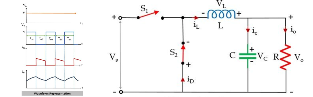
The working principle of buck convertors is by taking an input voltage and using interal MOSFETs to switch the voltage on and off really quickly. The effect of this is that the voltage, on average, is somewhere between the input voltage and ground. The output voltage depends the ratio of how long the voltage is on versus off (the duty cycle), which in these chips case is set by two feedback resistors. The choppy on/off signal is smoothed by a series inductor and a parallel capacitor; the series inductor resists current changes and smooths out the choppy PWM waveform, and the parallel capacitor helps regulate the voltage by allowing ripples to pass to ground.

This is a good article if interested.
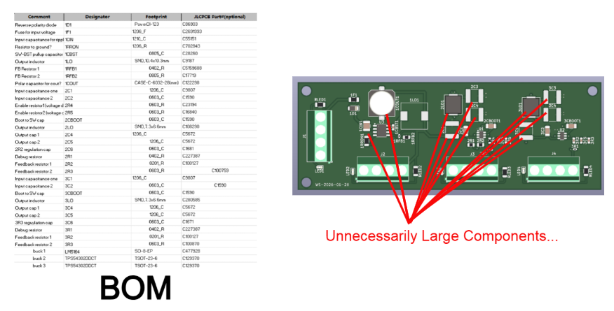
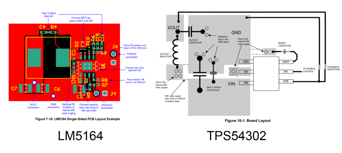
I designed the board in KiCAD. The layout was done by referencing the datasheets for the LM5164 and TPS54302. For both, the idea was the same – keep the boost capacitor and feedback resistors close to the chips. This is to prevent noise and parasitic capacitance, which could hurt performance.
 Layout References
With the references in mind, I used JLCPCB’s online part database to spec out all of the components needed. I oversized almost everything as this was one of my first SMD PCBs and I wanted to make sure that if I made any mistakes, I wouldn’t destroy all the components. That is why there are some comically large capacitors/indictors, like here. For my ESC implementation, I replaced a lot of the 1206 and 0805 components with 0402 and 0603s so I could save space.

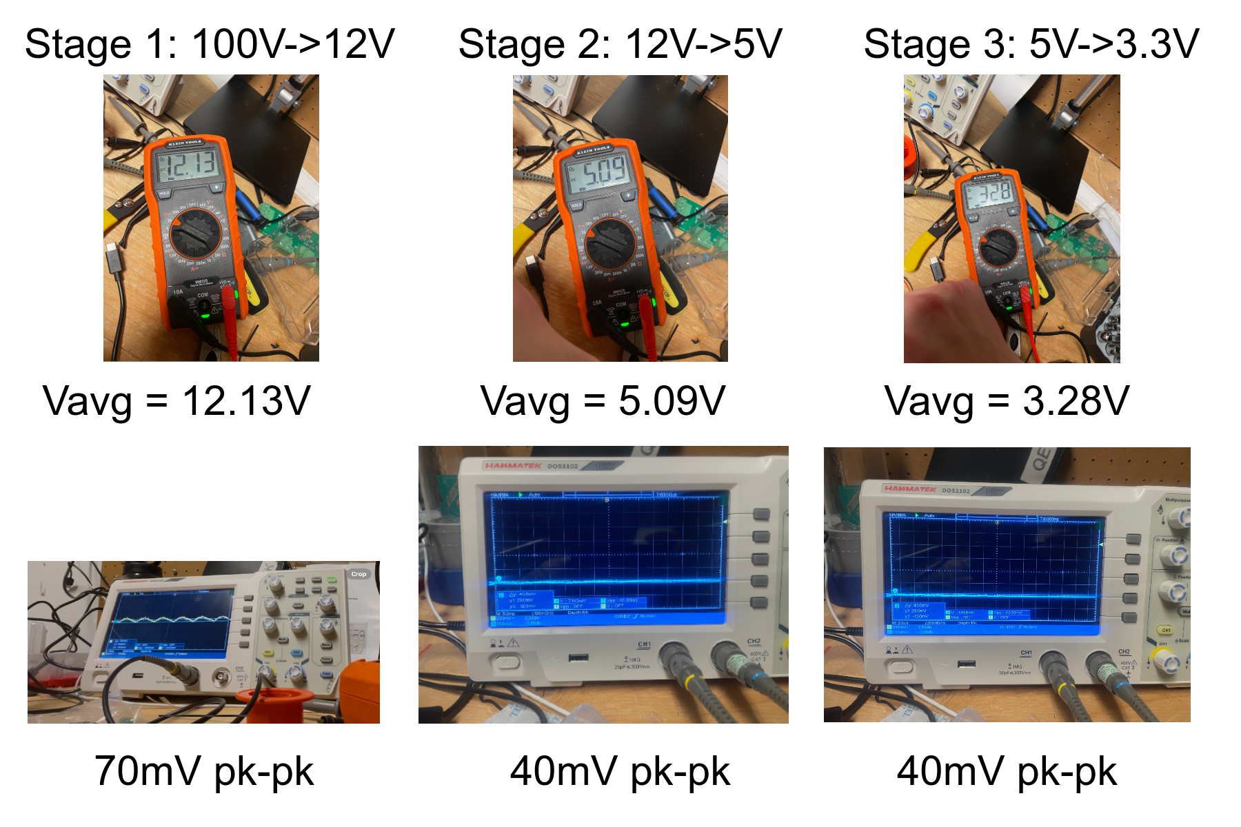
I used an oscilloscope to measure the output ripple for each stage. The LM5164 (12V) stage had much more ripple than i expected; about 70mV pk-pk. The other two stages were much smaller, around 40mV pk-pk.

Takeaways
I’m glad I did this project, heres what I learned:
- Trace length and component position are critical variables. Putting components far away from each other can lead to unwanted “impedance mismatches” that can cause signal reflections and unwanted noise. An example from this project is the placement of the inductor and output capacitors; as close as possible to the board, so minimizing the loop area and output ripple
This video gave some good insight
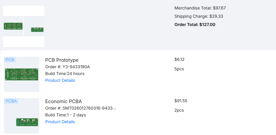
- PCB assembly is expensive. Getting the board made cost under $15, but getting a 3rd party solder components onto it cost $200. Using “Basic” instead of “Extended” parts is not always possible for circuit design but can keep costs lower.
 USD
USD
Related albums
Simple BB8
1 photo
Turreting Treat-Launching Catapult for my Dog
19 photos
Honda Canada Mfg. Open House 2025
1 photo